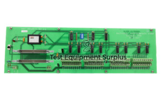
Description
The USRP-2952 is a model that boasts an array of impressive features suitable for a wide range of applications. It is identified by two part numbers, 783151-01 and 783927-01, designed to cater to various operational needs. One of the standout features of this model is its RF Frequency Range, which spans from 400 MHz to 4.4 GHz, offering a broad spectrum for diverse radio frequency applications.
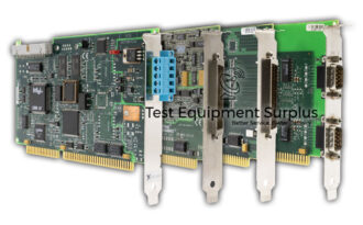
At its core, the USRP-2952 is powered by the Kintex-7 410T FPGA, a highly capable programmable logic device that ensures high performance and flexibility for custom applications. The device’s precision is enhanced by its GPS disciplined oscillator (OCXO) reference clock, ensuring accurate frequency synthesis and timing.
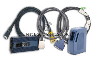
Connectivity options for the USRP-2952 are robust, featuring both Gigabit Ethernet and PCIe interfaces, facilitating easy integration into a variety of systems. For debugging purposes, a JTAG USB port is available, allowing developers to troubleshoot and program the FPGA with ease.
The device also includes general-purpose I/O ports, controlled by the FPGA, which provide additional flexibility for custom applications. These I/O ports can be used for a myriad of purposes, ranging from signal control to interfacing with other hardware components.
In terms of radio frequency capabilities, the USRP-2952 offers a Transceiver Instantaneous Bandwidth that comes standard at 40 MHz, with an optional extension up to 120 MHz. This feature ensures that the device can handle a wide bandwidth, making it suitable for high-data-rate applications.
The device includes two transmitter channels, each operating within the 400 MHz to 4.4 GHz range, providing dual-channel capability for complex operations. The transmitter gain range of 0 dB to 31.5 dB allows for precise control over signal strength, ensuring optimal performance across various conditions.
Moreover, the USRP-2952 has the
Question 1: What FPGA does the USRP-2952 use? Question 2: What is the RF range of the USRP-2952? Question 3: How many transmitter channels does the USRP-2952 have? Question 4: What interfaces does the USRP-2952 support? Question 5: What is the standard bandwidth of the USRP-2952?
Feature
Description
Model
USRP-2952
Part Numbers
783151-01, 783927-01
RF Frequency Range
400 MHz to 4.4 GHz
FPGA
Kintex-7 410T
Reference Clock
GPS disciplined oscillator (OCXO)
Connectivity
Gigabit Ethernet, PCIe
Debugging Port
JTAG USB port
General-purpose I/O
Controlled by FPGA
Transceiver Instantaneous Bandwidth
Standard: 40 MHz, Optional: 120 MHz
Transmitter Channels
Two 400 MHz to 4.4 GHz channels
Transmitter Gain Range
0 dB to 31.5 dB
Synchronization Capability
Ability to synchronize multiple NI USRP-2952 devices
Answer 1: Kintex-7 410T FPGA
Answer 2: 400 MHz to 4.4 GHz
Answer 3: Two
Answer 4: Gigabit Ethernet and PCIe
Answer 5: 40 MHz