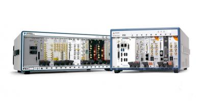
Description
The part number 781035-01 refers to the PXI-5691 model, which falls under the category of General Purpose RF Sig Conditioning. This device is described as a CCA, PXI-5691, RF AMPLIFIER, designed to enhance RF signals for a variety of applications. It is equipped with 2-Channel capability, allowing it to process two separate signals simultaneously.
The PXI-5691 operates within a frequency range of 50 MHz to 8.0 GHz, catering to a broad spectrum of RF applications. It features a gain path that includes one programmable and one fixed option, providing flexibility in signal amplification. For Channel 0, the maximum input power is typically +30 dBm, with a maximum reverse power of +20 dBm and a maximum output power of +25 dBm.
Channel 1 offers a gain range of +31.5 dB, with a gain step size of +0.5 dB. The maximum level settling time for Channel 1 is +4 µs, indicating the device’s efficiency in reaching a stable output level swiftly.
The power consumption of the PXI-5691 is distributed across different voltages, consuming 2.1 W at 3.3 Vdc, 6.9 W at 5 Vdc, 2.9 W at 12 Vdc, and 0.34 W at -12 Vdc. This detailed power usage information helps in planning the power supply requirements for integrating the PXI-5691 into various systems.
| Specification | Detail |
|---|---|
| Part Number | 781035-01 |
| Model | PXI-5691 |
| Category | General Purpose RF Sig Conditioning |
| Description | CCA, PXI-5691, RF AMPLIFIER |
| Channels | 2-Channel |
| Frequency Range | 50 MHz to 8.0 GHz |
| Gain Path | One programmable, one fixed |
| Maximum Input Power (CH 0) | +30 dBm typical |
| Maximum Reverse Power (CH 0) | +20 dBm maximum |
| Maximum Output Power (CH 0) | +25 dBm maximum |
| Gain Range (CH 1) | +31.5 dB |
| Gain Step Size (CH 1) | +0.5 dB |
| Maximum Level Settling Time (CH 1) | +4 µs |
| Power Consumption | 2.1 W at 3.3 Vdc, 6.9 W at 5 Vdc, 2.9 W at 12 Vdc, 0.34 W at -12 Vdc |


