Description
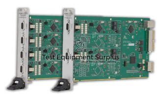
The NI USRP-2952 is a USRP Software Defined Radio Device designed for advanced radio applications. It features dual part numbers, 783151-01 and 783927-01, indicating different configurations or versions available for specific needs. As a product categorized under NI USRP, it stands out in the field of software-defined radio technology.
One of the key specifications of the USRP-2952 is its RF Frequency Range, which spans from 400 MHz to 4.4 GHz. This wide range allows for versatile applications in both commercial and research environments. The device is powered by a Kintex-7 410T FPGA, providing substantial processing power for complex signal processing tasks.
Accuracy and precision are ensured with the inclusion of a GPS disciplined oscillator as its reference clock. This feature guarantees high reliability in timing and frequency synchronization, making it suitable for applications requiring high levels of accuracy.
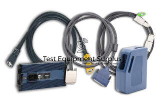
Connectivity options include Gigabit Ethernet and PCIe, offering flexibility in system integration and data transfer rates. Additionally, a JTAG USB port is available for debugging, enabling developers to troubleshoot and optimize their applications efficiently.
The USRP-2952 also boasts a general-purpose I/O controlled by the FPGA, allowing for custom interfacing and control schemes. This feature, along with the ability to synchronize multiple NI USRP-2952 devices, makes it an ideal choice for scalable and complex system setups.
In terms of RF capabilities, the device offers two transmitter channels covering the entire 400 MHz to 4.4 GHz range, with a transmitter gain range of 0 dB to 31.5 dB. The transceiver’s instantaneous bandwidth can be either the standard 40 MHz or an optional 120 MHz, depending on the application’s requirements.
| Spec | Detail |
|---|---|
| Part Number | 783151-01, 783927-01 |
| Category | NI USRP |
| Model | USRP-2952 |
| Description | USRP Software Defined Radio Device |
| RF Frequency Range | 400 MHz to 4.4 GHz |
| FPGA | Kintex-7 410T FPGA |
| Reference Clock | GPS disciplined oscillator |
| Connectivity | Gigabit Ethernet, PCIe |
| Debugging Port | JTAG USB |
| General-purpose I/O | Controlled by FPGA |
| Channel Count (Synchronization) | Can synchronize multiple NI USRP-2952 devices |
| Transceiver Instantaneous Bandwidth | Standard: 40 MHz, Optional: 120 MHz |
| Transmitter Channels | Two 400 MHz to 4.4 GHz channels |
| Transmitter Gain Range | 0 dB to 31.5 dB |
Question 1: What FPGA is used in the USRP-2952?
Answer 1: Kintex-7 410T FPGA
Question 2: What range does the RF frequency of USRP-2952 cover?
Answer 2: 400 MHz to 4.4 GHz
Question 3: What types of connectivity does the USRP-2952 offer?
Answer 3: Gigabit Ethernet and PCIe
Question 4: Can the USRP-2952’s reference clock be termed reliable?
Answer 4: Yes, uses a GPS disciplined oscillator.
Question 5: What is the max transmitter gain available on the USRP-2952?
Answer 5: 31.5 dB