Description
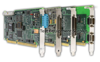
The NI PCI-7813R is identified by its part number 192463A-03 (779370-01) and falls under the category of PC-based R Series. This model, PCI-7813, is described as an NI PCI-7813R 3M Gate Digital RIO with 160 digital I/Os. It is built around a 3M Gate Virtex-II FPGA, making it a powerful solution for digital signal processing and complex control applications.
This device boasts 160 Digital I/Os, providing ample connectivity for a wide range of digital devices. It also includes 28,672 flip-flops and the same number of 4-input LUTs (Look-Up Tables), enhancing its capability to perform various logic operations efficiently. Additionally, the card is equipped with 96 multipliers (18 x 18), which are crucial for high-speed arithmetic operations.
Embedded within the FPGA is 1,728 Kbits of block RAM, enabling the storage of large amounts of data for quick access by the FPGA during operation. The device operates with a minimum sampling period of 5 ns and supports a minimum input pulse width of 25 ns and a minimum output pulse width of 12.5 ns, ensuring precise timing for all digital signals. It is compatible with various logic levels, including TTL, 3.3 V, and 5 V, offering versatility in connecting different types of digital devices.
The PCI-7813R operates at a maximum clock rate of 40 MHz, providing a balance between high-speed operation and power efficiency. Speaking of power, it has a typical power consumption of 850 mA at +3.3V, making it an energy-efficient choice for many applications. This combination of features makes the NI PCI-7813R an excellent choice for users requiring a high-performance, versatile, and efficient digital I/O solution.
| Specification | Details |
|---|---|
| Part Number | 192463A-03 (779370-01) |
| Category | PC-based R Series |
| Model | PCI-7813 |
| Description | NI PCI-7813R 3M Gate Digital RIO (160 DIO) |
| FPGA | 3M Gate Virtex-II |
| Digital I/Os | 160 |
| Flip-Flops | 28,672 |
| 4-input LUTs | 28,672 |
| Multipliers (18 x 18) | 96 |
| Embedded Block RAM | 1,728 Kbits |
| Minimum Sampling Period | 5 ns |
| Minimum Input Pulse Width | 25 ns |
| Minimum Output Pulse Width | 12.5 ns |
| Logic Levels Compatibility | TTL, 3.3 V, 5 V |
| Maximum Clock Rate | 40 MHz |
| Typical Power Consumption | 850 mA at +3.
Question 1: What FPGA does the PCI-7813 use? Question 2: How many digital I/Os does the PCI-7813 have? Question 3: What is the max clock rate of the PCI-7813? Question 4: What levels of logic is the PCI-7813 compatible with? Question 5: How much block RAM is in the PCI-7813? |