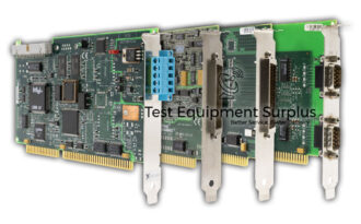
The National Instruments PCIe-7858 (Part Number: 786457-01) is a multifunction reconfigurable I/O device featuring a Kintex-7 325T FPGA, 8 analog input and output channels, 512 MB
The NI PCIe-7858, with Part Number 786457-01, features a powerful Kintex-7 325T FPGA and provides users with 8 analog input and output channels to accommodate diverse applications. Each analog input channel is equipped with a dedicated SAR ADC, ensuring precise data conversion and supporting input coupling for versatile signal processing. With 512 MB of DRAM and 48 digital I/O channels, this device stands out for complex tasks that require substantial memory and I/O capabilities.
Digital I/O channels are compatible with LVTTL and LVCMOS logic families and come with a default logic setting of 3.3V, which can be software-selected according to user requirements. To protect against potential damage, the device is designed with overvoltage protection of up to ±35 V maximum when powered on and ±42 V maximum when powered off.
The FPGA within the NI PCIe-7858 is robust, containing 407,600 flip-flops, 203,800 LUTs (Look-Up Tables), and 16,020 kbits of embedded block RAM, all of which contribute to the device’s flexibility and performance in processing and handling data. It is capable of achieving a maximum theoretical data rate of 800 MB/s, making it an excellent choice for high-speed data acquisition and control applications.
Feature
Specification
Part Number
786457-01
FPGA
Kintex-7 325T
Analog Input Channels
8
Analog Output Channels
8
DRAM
512 MB
Digital I/O Channels
48
ADC Type
SAR ADC (dedicated per channel)
Input Coupling Supported
Yes
Overvoltage Protection (Powered On)
±35 V maximum
Overvoltage Protection (Powered Off)
±42 V maximum
Digital I/O Compatibility
LVTTL, LVCMOS
Default Logic Setting
3.3V
FPGA Flip-Flops
407,600
FPGA LUTs
203,800
FPGA Embedded Block RAM
16,020 kbits
Maximum Theoretical Data Rate
800 MB/s
Question 1: What are the input and output specifications and overvoltage protection limits of the NI PCIe-7858 with Part Number 786457-01? Answer 1: The NI PCIe-7858 uses Successive Approximation Register (SAR) analog-to-digital conversion for its analog input channels, and it offers overvoltage protection of up to ±35 V maximum when powered on and ±42 V maximum when powered off.
Question 2: What is the maximum overvoltage protection provided by the NI PCIe-7858 when it is powered off, and how does its embedded Kintex-7 325T FPGA contribute to its performance in high-speed data acquisition and control applications? Answer 2: The NI PCIe-7858 is equipped with a Kintex-7 325T FPGA, 8 analog input and output channels with dedicated SAR ADCs, 512 MB of DRAM, and 48 digital I/O channels compatible with LVTTL and LVCMOS logic families, featuring overvoltage protection of up to ±35 V when powered on and ±42 V when powered off, along with a robust FPGA architecture that includes 407,600 flip-flops, 203,
Question 3: What type of analog-to-digital conversion does the NI PCIe-7858 use for its analog input channels, and what are the overvoltage protection values when the device is powered on and off? Answer 3: The NI PCIe-7858 provides a maximum overvoltage protection of ±42 V when it is powered off, and its embedded Kintex-7 325T FPGA, with 407,600 flip-flops, 203,800 LUTs, and 16,020 kbits of embedded block RAM, contributes to its performance in high-speed data acquisition and control applications by offering substantial flexibility, data processing capabilities, and a maximum theoretical data rate of 800 MB/s.
Question 4: What type of ADC technology is utilized in the NI PCIe-7858’s analog input channels, and what is its significance for data conversion? Answer 4: The NI PCIe-7858 with Part Number 786457-01 features 8 analog input and output channels, each with a dedicated SAR ADC for precise data conversion, and offers overvoltage protection of up to ±35 V maximum when powered on and ±42 V maximum when powered off.
Question 5: Based on the detailed description, what are the key features and protections provided by the NI PCIe-7858 to support its suitability for complex and high-speed data acquisition and control applications? Answer 5: The NI PCIe-7858’s analog input channels utilize Successive Approximation Register (SAR) ADC technology, which is significant for data conversion as it ensures precise and quick analog-to-digital conversion, allowing for accurate signal processing across the device’s multiple channels.